
Laminated Bus Bar
Laminated bus bars stack conductive layers with dielectric films to create compact, low-inductance power distribution for inverters, drives, and high-current DC links. Partsproto fabricates multi-layer copper or aluminum laminated assemblies to your layer count, hole pattern, and insulation plan—helping power electronics designers cut loop area versus discrete cabling while staying within a practical mid-size manufacturing process.
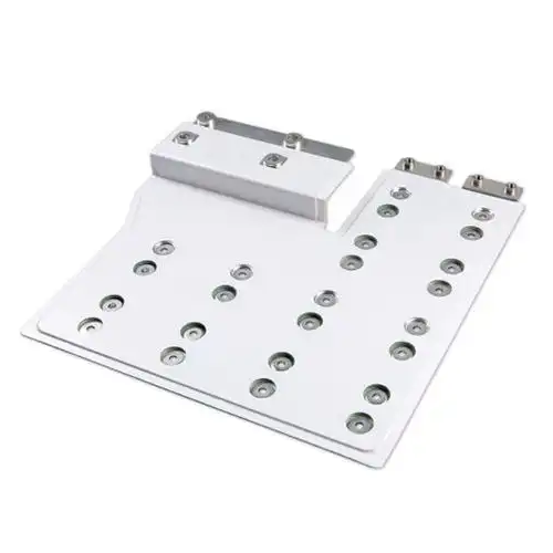
What laminated bus bars are
A laminated bus bar is a multi-layer conductor assembly: copper or aluminum sheets separated by dielectric films, pressed into a rigid sandwich with plated or bare terminals emerging at defined locations. The wide, flat, closely spaced layers reduce loop inductance compared with spaced cables or distant rigid bars.
That low inductance matters in fast-switching power electronics—IGBT and MOSFET stages see smaller voltage overshoot when DC link inductance drops. Laminated buses also tidy mechanical layout inside inverter and drive cabinets.
Partsproto builds laminated bars as custom fabrications. Layer count, dielectric choice, and edge sealing follow your design; we provide manufacturing DFM rather than claiming a one-size catalog stack.
Laminated buses can also embed multiple voltage domains—DC+/DC−, brake chopper, and auxiliary—in one mechanical assembly, cutting connector count. That only works when the stack drawing is unambiguous about which layer emerges where.
How laminated bars are made
Conductor layers are cut and cleaned; dielectric films are cut with appropriate overlaps and cutouts. Layers are stacked in sequence, registered to hole patterns, then pressed and cured or bonded per the dielectric system.
Edges may be sealed or covered to protect dielectric and improve creepage. Terminals are plated when specified. Complex designs add stepped layers, embedded sensors keep-outs, or asymmetric stacks for multi-voltage systems.
Inspection includes layer registration, thickness, hole positions, insulation integrity checks, and visual edge quality. Share voltage class and partial-discharge expectations if they affect dielectric selection.
Registration holes and tooling pins keep layers aligned through press. After bonding, excess dielectric is trimmed and edges finished so creepage paths match the design intent.
Design and ordering tips
Provide a layer stack drawing: conductor thickness per layer, dielectric type and thickness, terminal map, and any rivets or fasteners through the stack. Ambiguous stack-ups are the main cause of requotes.
Laminated vs solid: choose laminated when inductance and packaging density matter; choose solid when the geometry is simple and inductance is not critical.
RFQ at /contact with stack drawings and quantity. Laminated parts usually need longer lead time than single-layer bars.
Thermal vias or heatsink interfaces on laminated bars need early discussion—dielectric films are thermal resistors. If continuous current is high, plan cooling explicitly rather than assuming copper area alone is enough.
Laminated bus bars and power electronics DFM
Device footprints change—new IGBT modules shift terminal patterns. Laminated bars should be revision-controlled with the power stage BOM. We recommend naming the stack revision on both the bar drawing and the converter assembly drawing.
Partial discharge and creepage at edges are design responsibilities. Manufacturing can keep edges clean and sealed to the print, but dielectric thickness and overlap must be chosen for the voltage and environment by your power designer.
Prototyping laminated bars costs more per piece than solid flats, yet iterating inductance early often saves device failures later. Budget a pilot stack before freezing the enclosure.
Provide stack-up, terminal map, and quantity at /contact. Ask for DFM comments on press feasibility and edge treatment.
Partsproto builds laminated bus bars for power electronics teams that need custom stacks without pretending every project is a mega-OEM frame contract. Clear stack drawings and prototype-friendly lots are the entry path; production repeats follow the frozen revision.
Laminated stack checklist
Deliver a layer-by-layer stack: conductor metal and thickness, dielectric type and thickness, terminal emergence map, and edge treatment notes.
Include voltage class context and continuous current so DFM can sanity-check thermal and creepage assumptions—without replacing your power designer’s calculations.
Plan prototype and production quantities on one RFQ. Laminated tooling and press recipes benefit from knowing the follow-on volume.
Send stack drawings via /contact; Partsproto will comment on press feasibility and registration before you commit enclosure cutouts to the laminated outline.
Key Features
Discover the unique characteristics and advantages of Laminated Bus Bar
Multi-layer low-inductance layout
Wide parallel layers cut loop area for faster switching power stages.
Compact power density
Replaces bulky cable harnesses in inverter and drive cabinets.
Copper or aluminum layers
Material per layer chosen for conductivity, weight, and cost.
Custom layer counts
Typical stacks from a few layers up to denser multi-voltage designs within process limits.
Integrated terminal patterns
CNC-aligned holes and pads for devices, capacitors, and contactors.
Edge and dielectric protection
Sealing and cover options to protect insulation at the perimeter.
Technical Specifications
Detailed specifications for Laminated Bus Bar
Materials
Dimensions
Layers: 2 to 10 (typical range)
Thickness: 1 mm to 15 mm per conductor layer (typical)
Width: 20 mm to 500 mm (typical)
Finish Options
Applications
Explore the various applications where Laminated Bus Bar excels
Motor drives and inverters
DC link and output stage connections with controlled inductance.
Renewable power converters
Solar and storage inverters needing dense DC buswork.
UPS power stages
Compact laminated links between batteries, converters, and outputs.
Industrial power electronics
Welding, plating, and process supplies with fast switching.
EV power electronics
Onboard and offboard chargers and traction inverters (non-regulated statement).
Multi-voltage distribution
Stacked layers carrying different potentials in one assembly.
Advantages
- •Lower inductance than spaced cables
- •Cleaner mechanical packaging
- •Custom stacks for multi-voltage systems
- •Supports copper and aluminum strategies
- •Terminal patterns matched to devices
- •Useful from prototypes to production volumes
Limitations
- •Higher cost and longer lead time than solid bars
- •Stack design mistakes are expensive to fix
- •Thermal design still required for continuous current
- •Field repair of dielectric damage is limited
Frequently Asked Questions
Find answers to common questions about Laminated Bus Bar
How many layers can you build?
Many designs fall in a 2–10 layer practical range depending on thickness, dielectric, and press capability. Extreme stacks need individual review.
Why laminated instead of solid copper?
Laminated stacks reduce inductance and can integrate multiple potentials. Solid bars are simpler and cheaper when inductance is not critical.
What dielectric materials are used?
Film dielectrics suited to your voltage and temperature—specified on the stack drawing. We source to the callout rather than substituting silently.
Can terminals be plated?
Yes—tin or silver on exposed terminals is common. Define which faces and holes need plating.
What files are required?
Layer stack, outline, hole chart, material list, and finish notes. STEP models help for interference checks.
Lead time?
Longer than single-layer bars because of stacking and bonding. Prototype schedules are quoted explicitly.
Do you do partial discharge testing?
Advanced electrical tests can be discussed when scoped; many customers perform system-level PD on the finished converter. Ask on the RFQ. Keep fastener torque within the stack’s rated practice—over-torque can crush dielectric locally and create creepage weak points that appear only after thermal cycling.
Ready to Get Started?
Contact us today to discuss your Laminated Bus Bar requirements and get a customized solution for your application.